
Si Piezosensor for Angle Control of Piezoelectric MEMS Micromirror
Date:
MEMS, Piezoresistors, Micromirror, Sensor Design, Finite Element Analysis, Fabrication
Introduction
MEMS (Micro-Electro-Mechanical Systems) micromirrors are critical components in optical applications such as laser scanning displays, LiDAR systems, and biomedical imaging. Two-dimensional (2D) piezoelectric micromirrors require precise angle control on both axes, but the slow axis often lacks effective feedback sensing due to mechanical design constraints.
Project Objective: Design and fabricate an integrated Si piezoresistive angle sensor for the slow axis of a 2D piezoelectric micromirror to enable closed-loop feedback control and improve positioning accuracy.
Impact: This research contributes to the development of high-precision optical MEMS devices with applications in autonomous vehicles (LiDAR), medical imaging (endoscopy), and augmented reality displays.
Methods
Sensor Design
I designed a piezoresistive angle sensor structure specifically for the slow axis of the 2D piezoelectric micromirror:
Design Approach:
- Integrated Si piezoresistors at the hinge locations where mechanical stress is maximized during mirror rotation
- Optimized sensor geometry to balance sensitivity and mechanical robustness
- Designed two prototype structures: cantilever and meandering configurations for comparative analysis
Finite Element Analysis (FEA):
- Performed stress distribution analysis using COMSOL Multiphysics
- Simulated piezoresistive output under various deflection angles
- Validated sensor placement and geometry optimization
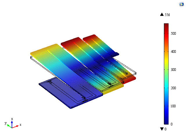
Finite element analysis simulation showing stress distribution during mirror deflection
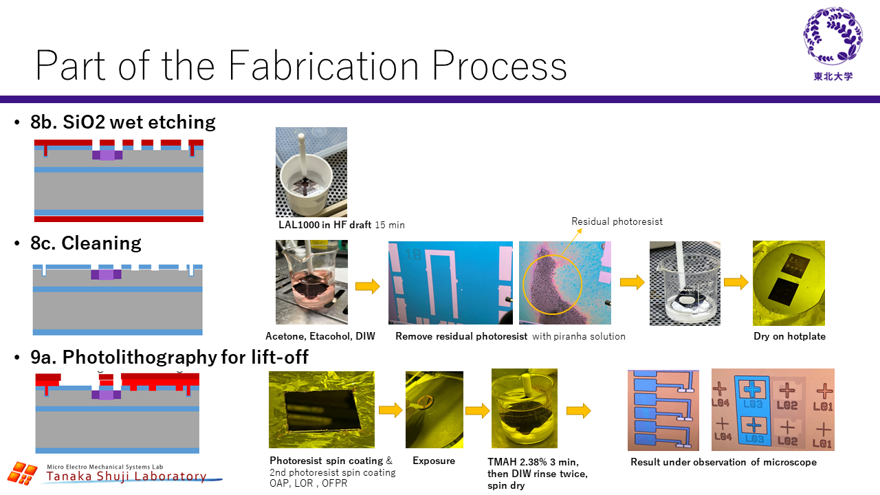
Fabrication Process
I gained hands-on experience with the complete MEMS fabrication workflow at Tohoku University’s cleanroom facility:
Silicon-on-Insulator (SOI) Wafer Processing:
- Deposition: Thin-film metal deposition for electrical contacts
- Photolithography: UV exposure and pattern transfer using photoresist
- Doping: Boron diffusion to create piezoresistive regions
- Etching: Deep reactive ion etching (DRIE) to define device structure
- Dicing: Wafer separation into individual device chips
- Wire Bonding: Electrical connection to package pins
- Packaging: Device encapsulation and protection
Fabrication Techniques:
- Doped wiring technique for creating low-resistance interconnects
- Precision alignment for multi-layer patterning
- Quality control and inspection at each process step
Fabricated MEMS devices showing cantilever and meandering piezoresistor structures
Results
Device Characterization
Successfully fabricated and characterized multiple prototype devices:
Output Testing:
- Measured voltage output from piezoresistors under controlled deflection
- Compared experimental results with FEA simulation predictions
- Evaluated sensor linearity and sensitivity across operating range
Key Findings:
- Piezoresistive sensors successfully detected angular deflection of the slow axis
- Output signal showed good correlation with simulation predictions
- Meandering structure demonstrated enhanced sensitivity compared to simple cantilever design
- Sensor integration did not significantly impact mirror mechanical performance
Design Validation
The comparative analysis between simulation and experimental results validated the effectiveness of:
- FEA-driven design optimization
- Piezoresistor placement strategy
- Fabrication process flow
Discussion
Technical Insights
Piezoresistive Sensing Advantages:
- Simple electrical interface compared to capacitive or optical methods
- Direct integration into MEMS structure without additional components
- Robust operation in challenging environmental conditions
Design Trade-offs:
- Sensitivity vs. mechanical stiffness: Higher sensitivity requires thinner structures but may compromise mechanical robustness
- Sensor placement: Must balance maximum stress location with manufacturing constraints
- Temperature effects: Piezoresistors exhibit temperature-dependent behavior requiring compensation
MEMS Fabrication Learning
This project provided comprehensive understanding of MEMS fabrication:
- Cleanroom protocols and contamination control
- Process parameter optimization for each fabrication step
- Troubleshooting and yield improvement strategies
- The critical importance of precision and cleanliness in microfabrication
Challenges Overcome:
- Achieving uniform doping concentration across the wafer
- Preventing structure damage during DRIE
- Ensuring reliable wire bond connections on microscale pads
My Role & Contributions
As an undergraduate research assistant in the S. Tanaka Laboratory, I:
✓ Designed the piezoresistive sensor structure and performed FEA simulations
✓ Executed the complete fabrication process from wafer processing to packaging
✓ Conducted experimental characterization and data analysis
✓ Performed comparative analysis between simulation and experimental results
✓ Gained proficiency in cleanroom operations and MEMS fabrication techniques
This research was conducted under the supervision of Prof. Shuji Tanaka and Assist. Prof. Andrea Vergara at Tohoku University’s Micro-Nano Systems Engineering Laboratory.
Technical Skills Gained: MEMS Design, Finite Element Analysis (COMSOL), Cleanroom Fabrication, Photolithography, Thin-Film Deposition, Wire Bonding, Device Characterization
Conclusion
This project successfully demonstrated the design and fabrication of integrated Si piezoresistive angle sensors for 2D piezoelectric MEMS micromirrors. The sensors enable closed-loop feedback control of the slow axis, improving positioning accuracy for high-precision optical applications.
Key Achievements:
- Novel piezoresistive sensor design for slow-axis angle detection
- Complete hands-on MEMS fabrication experience from design to testing
- Validation of sensor performance through experimental characterization
- Enhanced understanding of the relationship between mechanical design and sensor sensitivity
This research experience provided foundational knowledge in MEMS engineering that continues to inform my current work in robotics and sensor systems.